SMD mounting: basics of soldering, PCB soldering and technology. Installation of SMD at home. SMD components (chip components) Smd this item consists of
Today we will talk about SMD components , which appeared due to progress in the field of radio electronics and we will touch a little on such a radio element as .
Surface Mounted Device or smd translated as - surface mount devices, i.e. a type of radio components that are soldered from the side of the tracks and contact pads directly to the board.

In modern electronics, it is difficult to find a circuit that would not use smd components . In terms of parameters, most smd parts are no different from ordinary parts, except for size and weight. Due to its compactness, it became possible to create complex electronic devices of small sizes, for example, a cell phone.

The convenience of such a transistor lies not only in its size, but also in the fact that in most cases the pinout of such elements is the same.

The construction of these planar transistors is shown below.

Like conventional transistors, planar transistors also have many types: field-effect, composite (Darlington), IGBT (bipolar, insulated gate), bipolar.
Features, advantages and disadvantages of using SMD components in modern computers, laptops, smartphones.
SMD components (chip components)- these are components of an electronic circuit printed on a printed circuit board (motherboard of a computer, laptop, tablet, smartphone, hard drive, etc.) using surface mount technology - SMT technology (English surface mount technology). That is, all electronic elements , which are "fixed" on the board in this way, are called SMD components (English surface mounted device).
For this type of installation, it is characteristic that, unlike the older through-hole technology (when a hole is drilled in the textolite for an electronic component: a transistor, resistor, capacitor), SMD components are located much more compactly on the printed circuit board. The components themselves are much smaller.
If you pay attention to a modern laptop motherboard, you can see that it is SMD components that make up the bulk of the parts on the board - there are a lot of them and they are very heaped (small multi-colored squares and rectangles of gray, black), and on both sides of the textolite.
The motherboard of a tablet or smartphone is made exclusively using technology SMT (surface mount) and SMD elements, since there is no space and need for through-hole mounting.
In desktop motherboards, both mounting technologies are most often used. The contacts of the components (electrolytic capacitors in this case) are inserted into special holes in the motherboard and soldered on the reverse side.

Benefits of SMD Components and Surface Mount
- Smaller SMD components compared to through-hole elements;
- Significantly higher board density;
- Higher density of tracks (connections) on textolite;
- Components can be located on both sides of the board;
- Small errors during SMT mounting (soldering) are corrected automatically by the surface tension of molten tin (lead);
- Better resistance to mechanical failure due to vibration;
- Lower resistance and inductance;
- There is no need to drill holes and, as a result, a lower initial cost of production (economic effect);
- More adapted to automated assembly. Some automatic lines are capable of placing more than 136,000 components per hour;
- Many SMD components cost less than their through-hole counterparts;
- Suitable for devices with a very low profile (height). The printed circuit board can be used in an enclosure that is only a few millimeters thick
disadvantages
- Higher requirements for the production base and equipment;
- Low maintainability and higher requirements for repair specialists;
- Not suitable for mounting connectors and connectors, especially when used in the case of frequent disconnections and connections;
- Not suitable for use in high power and high load equipment
In our turbulent age of electronics, the main advantages of an electronic product are small dimensions, reliability, ease of installation and dismantling (equipment disassembly), low energy consumption and convenient usability ( from English- the convenience of use). All these advantages are by no means possible without surface mount technology - SMT technology ( S face M ount T echnology), and of course, without SMD components.
What are SMD components
SMD components are used in absolutely all modern electronics. SMD ( S face M ounted D evice), which is translated from English as “surface-mounted device”. In our case, the surface is a printed circuit board, without through holes for radio elements:
In this case, SMD components are not inserted into the board holes. They are soldered onto the contact tracks, which are located directly on the surface of the printed circuit board. In the photo below, there are tin-colored contact pads on the board of a mobile phone that used to have SMD components.

Advantages of SMD components
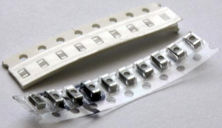
The biggest advantage of SMD components is their small size. In the photo below, simple resistors and:


Due to the small dimensions of SMD components, developers have the opportunity to place a larger number of components per unit area than simple output radio elements. Consequently, the mounting density increases and, as a result, the dimensions of electronic devices are reduced. Since the weight of the SMD component is several times lighter than the weight of the same simple output radio element, the mass of the radio equipment will also be many times lighter.

SMD components are much easier to desolder. For this we need a hair dryer. How to solder and solder SMD components, you can read in the article how to solder SMD correctly. Soldering them is much more difficult. In factories, they are placed on a printed circuit board by special robots. No one welds them manually in production, except for radio amateurs and radio equipment repairmen.
Multilayer boards
Since in equipment with SMD components there is a very dense installation, there should be more tracks in the board. Not all tracks fit on the same surface, so printed circuit boards make multilayer. If the equipment is complex and has a lot of SMD components, then there will be more layers in the board. It's like a layered cake. The printed tracks connecting the SMD components are located right inside the board and cannot be seen in any way. An example of multilayer boards is mobile phone boards, computer or laptop boards (motherboard, video card, RAM, etc.).
In the photo below, the blue board is Iphone 3g, the green board is the computer motherboard.


All radio repairers know that if you overheat a multilayer board, it will swell up with a bubble. In this case, the interlayer connections are torn and the board becomes unusable. Therefore, the main trump card when replacing SMD components is the right temperature.
On some boards, both sides of the printed circuit board are used, while the mounting density, as you understand, is doubled. This is another plus of SMT technology. Oh yes, it is also worth considering the fact that the material for the production of SMD components takes many times less, and their cost in mass production in millions of pieces costs, literally, a penny.
Main types of SMD components
Let's look at the main SMD elements used in our modern devices. Resistors, capacitors, low-value inductors, and other components look like ordinary small rectangles, or rather, parallelepipeds))

On boards without a circuit, it is impossible to know whether it is a resistor, or a capacitor, or even a coil. The Chinese mark as they want. On large SMD elements, they still put a code or numbers to determine their belonging and denomination. In the photo below, these elements are marked in a red rectangle. Without a diagram, it is impossible to say what type of radio elements they belong to, as well as their denomination.

Sizes of SMD components can be different. Here is a description of the sizes for resistors and capacitors. Here, for example, is a rectangular yellow SMD capacitor. They are also called tantalum or simply tantalum:

And this is what SMD looks like:


There are also these types of SMD transistors:

Which have a large denomination, in the SMD version they look like this:


And of course, how could it be without microcircuits in our age of microelectronics! There are a lot of SMD chip package types, but I mainly divide them into two groups:
1) Microcircuits, in which the leads are parallel to the printed circuit board and are located on both sides or along the perimeter.

2) Microcircuits, in which the conclusions are located under the microcircuit itself. This is a special class of microcircuits called BGA (from English ball grid array- an array of balls). The conclusions of such microcircuits are simple solder balls of the same size.
In the photo below, the BGA microcircuit and its reverse side, consisting of ball leads.

BGA chips are convenient for manufacturers in that they greatly save space on the printed circuit board, because there can be thousands of such balls under any BGA chip. This greatly simplifies the life of manufacturers, but does not make life easier for repairmen.
Summary
What do you use in your designs? If your hands are not shaking, and you want to make a small radio bug, then the choice is obvious. But still, in amateur radio designs, dimensions do not particularly play a big role, and soldering massive radio elements is much easier and more convenient. Some radio amateurs use both. Every day more and more new chips and SMD components are being developed. Smaller, thinner, more reliable. The future, unambiguously, belongs to microelectronics.
Modern radio equipment is built mainly only on the so-called chip components, these are chip resistors, capacitors, microcircuits, and so on. The output radio components that we used to solder from old TVs and tape recorders and that radio amateurs usually use to assemble their circuits and devices are less and less used in modern radio equipment.
What are the advantages of using such chip elements? Let's figure it out.
The advantages of this type of installation
Firstly, the use of chip components significantly reduces the size of finished printed circuit boards, their weight is reduced, as a result, this device will require a small compact case. So you can assemble very compact and miniature devices. The use of chip elements makes it possible to save a printed circuit board (fiberglass), as well as ferric chloride for etching them, in addition, you do not have to spend time drilling holes, in any case, it does not take much time and money.
Boards made in this way are easier to repair and easier to replace the radio elements on the board. You can make double-sided boards, and place elements on both sides of the board. Well, and saving money, because the chip components are cheap, and it is very profitable to buy them in bulk.
First, let's define the term surface mount, what does it mean? Surface mounting is a technology for the production of printed circuit boards, when radio components are placed on the side of the printed tracks, it is not necessary to drill holes to place them on the board, in short, this means "surface mounting". This technology is the most common today.
In addition to the pros, there are of course also cons. Boards assembled on a chip components are afraid of bends and bumps, because. after that, radio components, especially resistors with capacitors, simply crack. Chip components do not tolerate overheating when soldering. From overheating, they often crack and microcracks appear. The defect does not manifest itself immediately, but only during operation.
Types and types of chip radio components
Resistors and Capacitors
Chip components (resistors and capacitors) are primarily divided by size, there are 0402 - these are the smallest radio components, very small, such are used, for example, in cell phones, 0603 - also miniature, but slightly larger than the previous ones, 0805 - are used, for example, in motherboards boards, the most popular, then 1008, 1206 and so on.
Resistors:

Capacitors:
Below is a more table showing the dimensions of some elements:
- 1.0×0.5mm
- 1.6×0.8mm
- 2.0×1.25mm
- 3.2×1.6mm
- 4.5×3.2mm
All chip resistors are marked with a code, although a method for decoding these codes is given, many still do not know how to decipher the values of these resistors, in connection with this I painted the codes of some resistors, take a look at the table.

Note: There is an error in the table: 221 "Ohm" should be read as "220 Ohm".
As for capacitors, they are not labeled or labeled in any way, so when you buy them, ask the seller to sign the tapes, otherwise you will need an accurate multimeter with a capacitance detection function.
transistors
Basically, radio amateurs use transistors of the SOT-23 type, I won’t talk about the rest. The dimensions of these transistors are as follows: 3 × 1.75 × 1.3 mm.

As you can see, they are very small, you need to solder them very carefully and quickly. Below is the pinout of the conclusions of such transistors:

The pinout for most transistors in such a package is exactly the same, but there are exceptions, so before soldering the transistor, check the pinout by downloading the datasheet for it. Such transistors in most cases are designated with one letter and 1 number.
Diodes and zener diodes
Diodes, like resistors with capacitors, come in different sizes, larger diodes are marked with a strip on one side - this is the cathode, but miniature diodes can differ in labels and pinouts. Such diodes are usually designated by 1-2 letters and 1 or 2 numbers.


Zener diodes, like diodes, are indicated by a strip on the edge of the case. By the way, because of their shape, they like to run away from the workplace, they are very nimble, and if they fall, you won’t find them, so put them, for example, in the lid of a rosin jar.
Microcircuits and microcontrollers
Microcircuits come in different cases, the main and commonly used types of cases are shown below in the photo. The worst case type is SSOP - the legs of these microcircuits are located so close that it is almost impossible to solder without snot, the nearest outputs stick together all the time. Such microcircuits need to be soldered with a soldering iron with a very thin tip, and preferably with a soldering dryer, if there is one, I described the method of working with a hairdryer and solder paste in this one.

The next case type is TQFP, the photo shows a case with 32 legs (ATmega32 microcontroller), as you can see, the case is square, and the legs are located on each side of it, the main disadvantage of such cases is that they are difficult to solder with a conventional soldering iron, but you can. As for the other types of cases, it is much easier with them.
How and with what to solder the chip components?
It is best to solder the radio component chip with a soldering station with a stabilized temperature, but if there is none, then it remains only a soldering iron, which must be turned on through the regulator! (without a regulator, most ordinary soldering irons have a tip temperature of 350-400*C). The soldering temperature should be around 240-280*C. For example, when working with lead-free solders having a melting point of 217-227*C, the temperature of the soldering tip should be 280-300°C. During the soldering process, excessively high tip temperature and excessive soldering time must be avoided. The tip of the soldering iron should be sharply sharpened, in the form of a cone or a flat screwdriver.
The printed tracks on the board must be irradiated and coated with an alcohol-rosin flux. It is convenient to support the chip component during soldering with tweezers or a fingernail, you need to solder quickly, no more than 0.5-1.5 seconds. First, one lead of the component is soldered, then the tweezers are removed and the second lead is soldered. The microcircuits must be very accurately aligned, then the extreme outputs are soldered and they are checked again to see if all the outputs exactly fall on the tracks, after which the remaining outputs of the microcircuit are soldered.
If adjacent pins stick together when soldering chips, use a toothpick, put it between the pins of the chip and then touch one of the pins with a soldering iron, it is recommended to use more flux. You can go the other way, remove the screen from the shielded wire and collect solder from the microcircuit pins.
Some photos from personal archive

Conclusion
Surface mounting allows you to save money and make very compact, miniature devices. With all its disadvantages that take place, the resulting effect undoubtedly speaks of the prospects and relevance of this technology.
SMD components (chip components)- these are electronic circuit components printed on a printed circuit board (motherboard of a computer, laptop, tablet, smartphone, hard drive, etc.) using surface mount technology - SMT technology (English surface mount technology). That is, all electronic elements that are “fixed” on the board in this way are called SMD components (surface mounted device).
For this type of installation, it is characteristic that, unlike the older through-hole technology (when a hole is drilled in the textolite for an electronic component: a transistor, resistor, capacitor), SMD components are located much more compactly on the printed circuit board. The components themselves are much smaller.
If you pay attention to a modern laptop motherboard, you can see that it is SMD components that make up the bulk of the parts on the board - there are a lot of them and they are very heaped (small multi-colored squares and rectangles of gray, black), and on both sides of the textolite. In the following figure, the SMD components are marked in red.
The motherboard of a tablet or smartphone is made exclusively using SMT (surface mount) technology and SMD elements, since there is no place and need for through mounting.
In desktop motherboards, both mounting technologies are most often used. In the figure below, through-hole elements are marked in green. The contacts of the components (electrolytic capacitors in this case) are inserted into special holes in the motherboard and soldered on the reverse side.

Benefits of SMD Components and Surface Mount
- Smaller SMD components compared to through-hole elements;
- Significantly higher board density;
- Higher density of tracks (connections) on textolite;
- Components can be located on both sides of the board;
- Small errors during SMT mounting (soldering) are corrected automatically by the surface tension of molten tin (lead);
- Better resistance to mechanical failure due to vibration;
- Lower resistance and inductance;
- There is no need to drill holes and, as a result, a lower initial cost of production (economic effect);
- More adapted to automated assembly. Some automatic lines are capable of placing more than 136,000 components per hour;
- Many SMD components cost less than their through-hole counterparts;
- Suitable for devices with a very low profile (height). The printed circuit board can be used in an enclosure that is only a few millimeters thick
disadvantages
- Higher requirements for the production base and equipment;
- Low maintainability and higher requirements for repair specialists;
- Not suitable for mounting connectors and connectors, especially when used in the case of frequent disconnections and connections;
- Not suitable for use in high power and high load equipment
Using materials: Surface-mount technology,